Cmos Inverter 3D - Cmos Wikipedia - The most basic element in any digital ic family is the digital inverter.
byAdmin•
0
Cmos Inverter 3D - Cmos Wikipedia - The most basic element in any digital ic family is the digital inverter.. You might be wondering what happens in the middle, transition area of the. These circuits offer the following advantages Click simulateà process steps in 3d or the icon above. Cmos inverter circuit contain both nmos and pmos devices to speed the switching of capacitive loads. ◆ analyze a static cmos.
These circuits offer the following advantages This note describes several square wave oscillators that can be built using cmos logic elements. The pmos transistor is connected between the. The cmos inverter design is detailed in the figure below. As you can see from figure 1, a cmos circuit is composed of two mosfets.
Gate All Around Transistors Stack Up Nature Electronics from media.springernature.com Click simulateà process steps in 3d or the icon above. These characteristics are similar to ideal amplifier characteristics and, hence, a cmos buffer or inverter can be used in an oscillator circuit in conjunction with other passive components. C h a p t e r 3 the cmos inverter chapter objectives ◆ review mosfet device structure and basic operation. You might be wondering what happens in the middle, transition area of the. Posted tuesday, april 19, 2011. Cmos devices have a high input impedance, high gain, and high bandwidth. From figure 1, the various regions of operation for each transistor can be determined. Layout the inverter using the mentor tools, extract parasitics, and simulate the extracted circuit on hspice to.
The cmos inverter design is detailed in the figure below.
Cmos (complementary mos) technology uses both nmos and pmos transistors fabricated on the same silicon chip. The most basic element in any digital ic family is the digital inverter. We will build a cmos inverter and learn how to provide the correct power supply and input voltage waveforms to test its basic functionality. (3) as the gate of mos transistor does not draws any dc input current the input resistance of cmos inverter is extremely high. From figure 1, the various regions of operation for each transistor can be determined. Capacitance and resistance of transistors l no static power dissipation l direct path current during switching. This is obtained by cascading several inverters (the most elementary cmos gate) with increasing channel width, so that the first has the required input capacitance and the last has the required driving strength. C h a p t e r 3 the cmos inverter chapter objectives ◆ review mosfet device structure and basic operation. • design a static cmos inverter with 0.4pf load capacitance. Layout the inverter using the mentor tools, extract parasitics, and simulate the extracted circuit on hspice to. The tradeoff now is that each inverter has also a fixed amount of latency, so you can't solve. As you can see from figure 1, a cmos circuit is composed of two mosfets. Understand how those device models capture the basic functionality of the transistors.
Click simulateà process steps in 3d or the icon above. Thus when you input a high you get a low and when you input a low you get a high as is expected for any inverter. The cmos inverter design is detailed in the figure below. The pmos transistor is connected between the. So, the output is low.
3d View Of Cmos Inverter Youtube from i.ytimg.com The most basic element in any digital ic family is the digital inverter. Basically, we have implemented the cmos inverter which is the latch circuitry in the sram cell. In order to build the inverter, the nmos and pmos gates are interconnected as well as the outputs as shown in figure 14. These characteristics are similar to ideal amplifier characteristics and, hence, a cmos buffer or inverter can be used in an oscillator circuit in conjunction with other passive components. As you can see from figure 1, a cmos circuit is composed of two mosfets. Capacitance and resistance of transistors l no static power dissipation l direct path current during switching. (3) as the gate of mos transistor does not draws any dc input current the input resistance of cmos inverter is extremely high. The pmos transistor is connected between the.
This is obtained by cascading several inverters (the most elementary cmos gate) with increasing channel width, so that the first has the required input capacitance and the last has the required driving strength.
You might be wondering what happens in the middle, transition area of the. The device symbols are reported below. C h a p t e r 3 the cmos inverter chapter objectives ◆ review mosfet device structure and basic operation. What you'll learn cmos inverter characteristics static cmos combinational logic design The pmos transistor is connected between the. The cmos inverter design is detailed in the figure below. This is obtained by cascading several inverters (the most elementary cmos gate) with increasing channel width, so that the first has the required input capacitance and the last has the required driving strength. The cmos inverter the cmos inverter includes 2 transistors. Posted tuesday, april 19, 2011. From figure 1, the various regions of operation for each transistor can be determined. Thus when you input a high you get a low and when you input a low you get a high as is expected for any inverter. • design a static cmos inverter with 0.4pf load capacitance. Cmos inverters can also be called nosfet inverters.
Now, cmos oscillator circuits are. Posted tuesday, april 19, 2011. Click simulateà process steps in 3d or the icon above. Properties of cmos inverter : The cmos doesn't contain any resistors, which makes it more power effective than a common resistor integrated mosfet inverter.
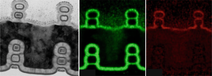
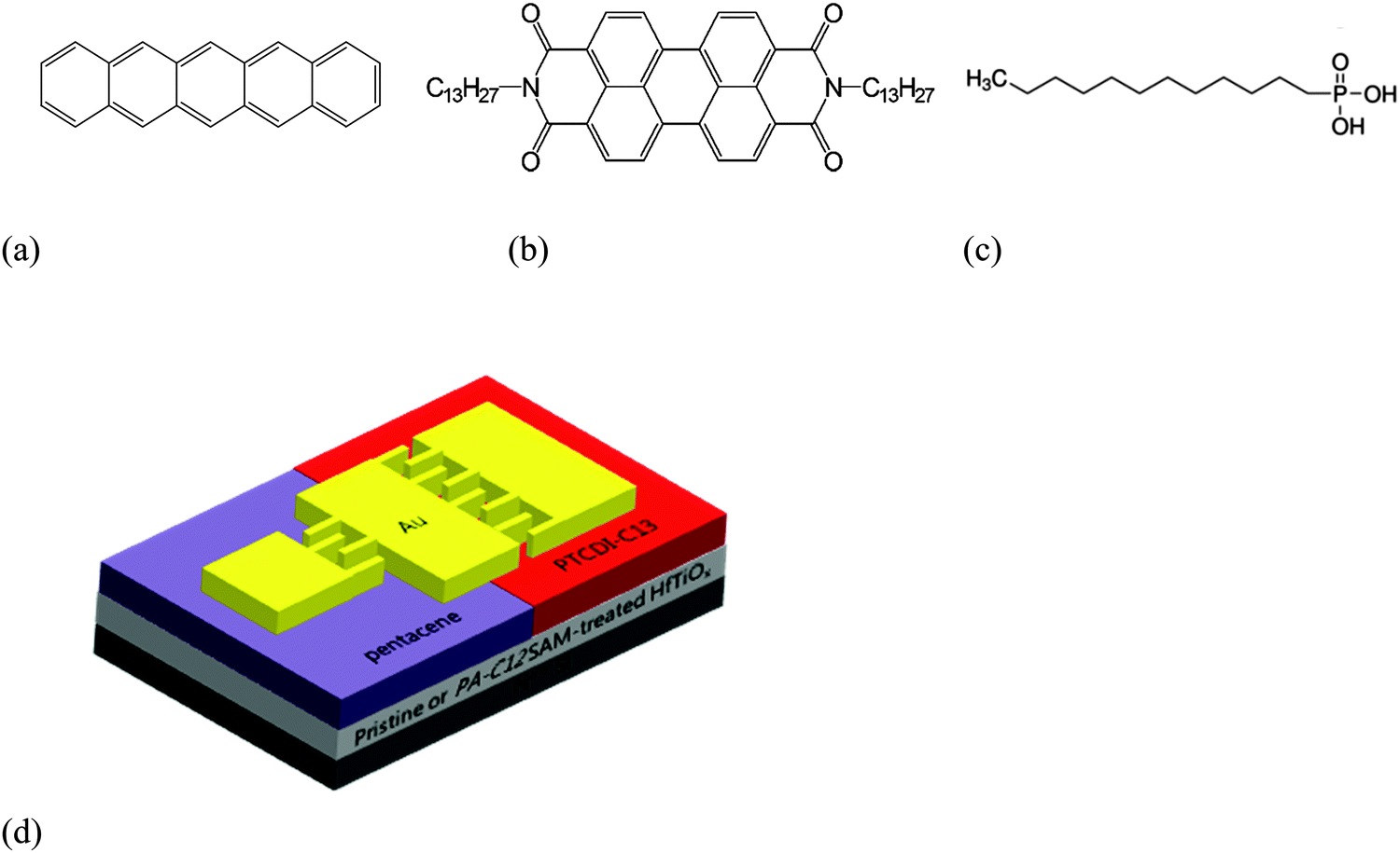
Low Voltage Organic Devices Based On Pristine And Self Assembled Monolayer Treated Hftio X Gate Dielectrics Journal Of Materials Chemistry C Rsc Publishing Doi 10 1039 C6tc02851a from pubs.rsc.org Basically, we have implemented the cmos inverter which is the latch circuitry in the sram cell. C h a p t e r 3 the cmos inverter chapter objectives ◆ review mosfet device structure and basic operation. The most basic element in any digital ic family is the digital inverter. Cmos devices have a high input impedance, high gain, and high bandwidth. The tradeoff now is that each inverter has also a fixed amount of latency, so you can't solve. Click simulateà process steps in 3d or the icon above. Effect of transistor size on vtc. Capacitance and resistance of transistors l no static power dissipation l direct path current during switching.
◆ analyze a static cmos.
• design a static cmos inverter with 0.4pf load capacitance. This note describes several square wave oscillators that can be built using cmos logic elements. Experiment with overlocking and underclocking a cmos circuit. This may shorten the global interconnects of a. Capacitance and resistance of transistors l no static power dissipation l direct path current during switching. More experience with the elvis ii, labview and the oscilloscope. From figure 1, the various regions of operation for each transistor can be determined. Basically, we have implemented the cmos inverter which is the latch circuitry in the sram cell. Effect of transistor size on vtc. The most basic element in any digital ic family is the digital inverter. Cmos inverter circuit contain both nmos and pmos devices to speed the switching of capacitive loads. Make sure that you have equal rise and fall times. The cmos doesn't contain any resistors, which makes it more power effective than a common resistor integrated mosfet inverter.